Power Electronics
Introduction
Switched mode power supplies (SMPS) date back to the mid-20th century. Before the advent of SMPS, linear regulators and transformers were commonly used to convert one voltage level to another. However, linear regulators are not very as efficient as SMPS, especially when the input and output voltages are significantly different [3]. The development of solid-state switch technology in the 1950s and 1960s, particularly with the introduction of the bipolar transistor, paved the way for SMPS designs and revolutionized digital power processing [4]. Switched mode power converters were developed primarily to address the limitations of traditional linear regulators below:
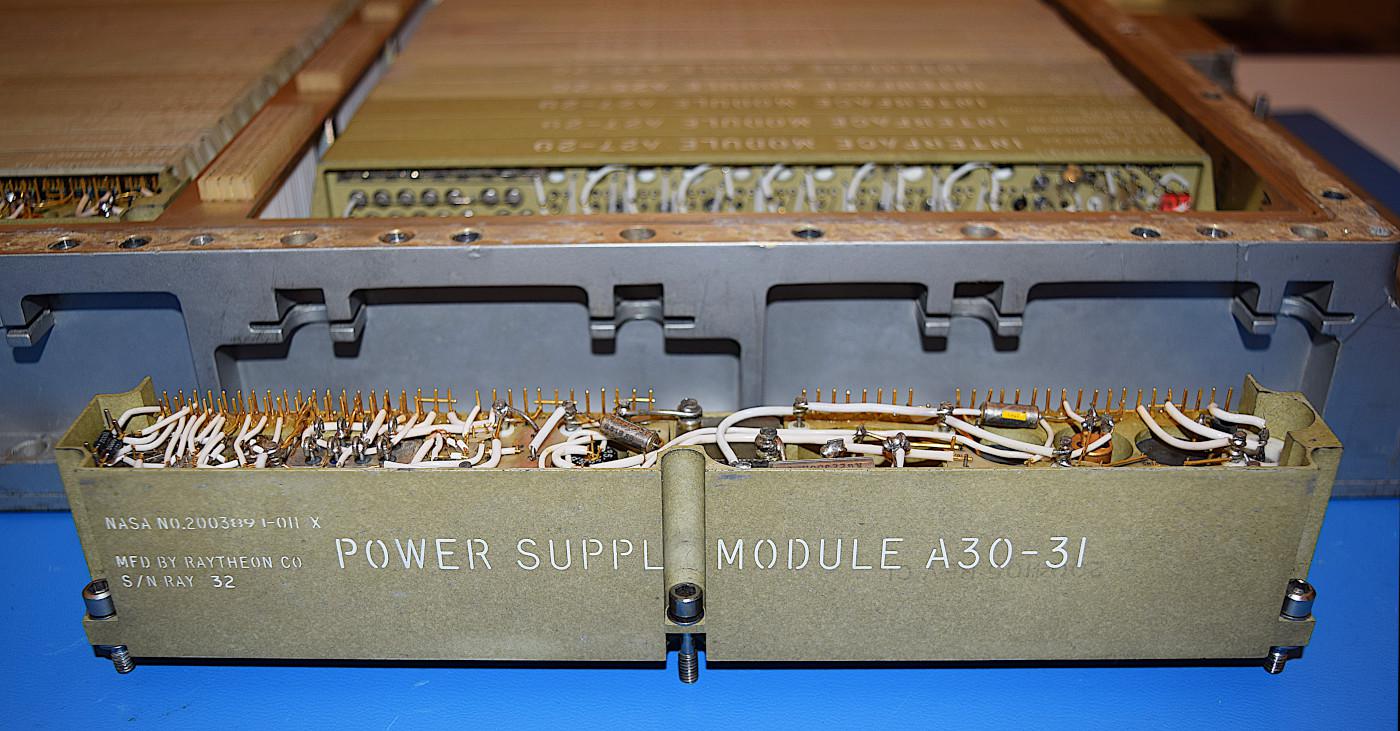
Figure 36 Apollo Guidance Computer (AGC) switched mode power supply. The left module is rated for 70 watts at 14 volts, and the right module proves 40 watts at 4 volts. Image courtesy of Ken Shirriff’s blog.
Efficiency: Linear regulators control the output voltage by dissipating excess power as heat, which can result in substantial energy losses—especially when the input voltage is much higher than the desired output. As a result, their efficiency often drops to around 30–40% cite{erickson2007fundamentals}. In contrast, switched-mode power supplies (SMPS) provide voltage regulation through high-frequency switching and energy storage components, enabling much higher efficiencies under a wide range of input–output voltage differences. Consequently, SMPS designs commonly exceed 90% efficiency.
Size and weight: Higher efficiency leads to less heat dissipation, allowing smaller heat sinks or, in some cases, eliminating the need for them entirely. This contributes to more compact designs. Additionally, as switching frequencies continue to increase, the size of filter elements that are needed to minimize switching ripple decreases significantly [5]. Consequently, this leads to power supplies that are both lighter and smaller.
Versatility: SMPS are remarkably versatile, capable of processing both AC and DC input signals while generating multiple output voltage levels. They can step up (boost) or step down (buck) voltage, invert polarity, change AC frequency, and convert between AC and DC. In the past, these functions required separate pieces of specialized equipment, such as transformers, dynamos, rotary converters, and vibrator-driven inverters. SMPS technology consolidates these functions into a single, compact design, offering unprecedented flexibility in power conversion cite{she2013review}.
Cost: While initial SMPS implementations may have been more expensive, technological advances and economies of scale have reduced the cost of components. Given the reduced need for large transformers and heat sinks, the overall cost of production for many SMPS solutions can be lower than that for equivalent linear power supplies. Additionally, as technology advanced, the switching frequencies of the SMPS increased, allowing smaller and cheaper filter components.
Improved performance: Digital power processing in switched-mode power supplies marks a significant evolution from traditional analog control methods. The use of sophisticated digital controllers and algorithms greatly improves the performance and versatility of the SMPS [1]. This approach allows precise control of power parameters, dynamic adjustment to fluctuations, and real-time monitoring and identification of faults. Furthermore, the incorporation of digital control simplifies the design phase, since changes can be made through software without the need for hardware modifications, making it faster and easier to tailor for various uses or changing environment.
Data Integration: With the rise of the Internet of Things (IoT) and smart devices, the SMPS digital power processing capability offers seamless interfacing and integration into larger digital ecosystems, laying the foundation for advanced energy management systems and optimization. The integration of digital technology into Switched-Mode Power Supplies paves the way for a data-driven approach to power management, revolutionizing how power systems are monitored, controlled, and optimized [6]. With digital SMPS, system parameters and performance metrics can be continuously collected and analyzed, enabling intelligent decision-making based on real-time data. This capability allows for dynamic adjustment of the power supply parameters to meet the varying demands of the load while optimizing efficiency and reliability [7]. In addition, the collected data can be used to predict system failures before they occur, schedule maintenance proactively, and ensure that the power supply operates consistently within its optimal parameters [8]. Furthermore, by using data analytics, designers can gain insight into usage patterns and system performance, informing future design improvements and customization tailored to specific application needs. This data-driven approach not only enhances the operational efficiency of power systems, but also significantly contributes to the advancement of smart and autonomous grids.
Structure of Power Converter
The power electronic converter can be defined as a multi-port system that facilitates energy exchange between different energy systems. These energy systems typically have different characteristics, such as voltage/current waveform, frequency, number of phases, or time-varying nature. Due to differences, these systems cannot be directly interfaced with each other and require an intermediary device to facilitate energy exchange [3]. In this work, we only consider converters that operate between two subsystems and limit the viable waveform to DC and AC.
We classify the converters into four primary categories based on the subsystems into which they interface.
DC/DC Converters: DC/DC converters are integral in portable electronics such as smartphones and laptops, ensuring that various components receive their required voltage levels [9]. In renewable energy systems, especially solar installations, DC/DC converters stabilize the variable outputs from solar panels. Automotive applications, particularly in electric vehicles, rely on these converters to efficiently distribute power to various component. In addition, they are essential in telecommunication infrastructures, optimizing the power distribution at base stations. Across industrial robotics, aerospace equipment, and even medical devices, DC/DC converters ensure stable and efficient power delivery.
AC/DC Converters (Rectifier): AC/DC converters or rectifiers are instrumental in transforming the alternating current (AC) from the main supply into the DC required by electronic devices [10]. They are ubiquitous in our daily lives, powering various household and industrial electronics, from laptop chargers and television sets to large-scale equipment in industrial settings. Beyond a simple power transformation, these converters ensure that the supplied DC voltage is stable and free from fluctuations, safeguarding sensitive electronics. The smartphone charger plugged into your wall outlet or the power brick connected to your computer are primary examples of AC/DC converter applications.
DC/AC Converters: DC/AC converters, commonly known as inverters, play a critical role in converting DC sources into AC voltage suitable for powering traditional electronic appliances and machinery [1]. These converters are quintessential in solar power installations, where the energy stored in batteries as DC must be converted to AC for household or grid use. Similarly, they are employed in uninterruptible power supplies (UPS) to provide AC power from stored DC energy during outages. Their ability to facilitate the use of AC devices in DC-dominated environments highlights their indispensable utility in modern power systems.
AC/AC Converters: AC/AC converters modify the magnitude and/or frequency of the AC voltage. Primary applications include variable-frequency drives (VFDs) for controlling the speed of AC motors in industrial and commercial environments, and to optimize energy consumption in HVAC systems and elevators [11, 12]. They are also used in power grid interconnections where the synchronization of different grids is necessary, in power quality improvement systems to manage voltage sags and surges, and in aircraft power systems to adjust the frequency. Furthermore, AC/AC converters facilitate power management in renewable energy systems, such as wind turbines, where the frequency can vary according to the speed of the wind.

Figure 37 Converters consist of two primary subsystems: the Power Unit and the Control Unit. The Power Unit encompasses high-power hardware designed to handle the processing of power. Meanwhile, the Control Unit is tasked with executing algorithms that manage the flow of power through the Power Unit.
Converters can be conceptually divided into two primary subsystems: the power unit and control subsystems as shown in Figure 37. The power unit primarily handles the high-power side of the converter, consisting of components such as switches, diodes, capacitors, and inductors that directly manage and modulate the energy flow. On the contrary, the control subsystem operates on the low-power side, comprising microcontrollers, sensors, and signal processors that dictate how the power unit should function. The power unit and the control subsystems of power electronics converters are interconnected through feedback sensor measurements and gate drive signals to ensure seamless operation. Sensors, often located within or close to the power unit, continuously monitor parameters such as voltage, current, etc. These sensors send this information to the control subsystem, which processes the data to make real-time decisions. Gate drive signals are generated based on the control subsystem’s decisions (often by a microcontroller or a DSP). These signals determine when and how the power unit’s switching elements (MOSFETs or IGBTs) should operate.
Note that the power unit handles high voltages and currents while the control subsystem operates at much lower levels, isolation is often necessary to ensure the safety and reliability of the system. Components such as optocouplers or digital isolators provide this isolation, especially when transmitting gate-drive signals or feedback.
Power Unit
The power unit in a converter is composed of several primary building blocks that facilitate the conversion of electrical energy. These building blocks include the following:
Switching elements: These are the core components responsible for managing the flow of electrical energy. Common switching devices include MOSFETs (Metal-Oxide-Semiconductor Field-Effect Transistors), IGBTs (Insulated-Gate Bipolar Transistors), BJTs (Bipolar Junction Transistors), and more recently GaN (Gallium Nitride) switches.
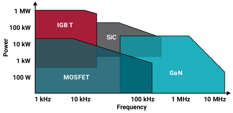
Figure 38 Trade-off between the switching frequency and power rating of different switching technologies. Image courtesy of the Texas Instruments.
IGBT is commonly used in medium- to high-power applications, typically in the range of a few hundred watts to several megawatts [13]. Its power rating is generally higher than that of MOSFETs for applications above 600V. However, IGBTs have a moderate switching frequency, typically less than 50kHz. In contrast, MOSFETs are suitable for lower-power applications, with power ratings typically in the range of a few watts to a few kilowatts. They excel in high-switching frequency applications, often exceeding 1MHz. GaN transistors, however, have emerged as a promising alternative for high-frequency and high-power applications [14]. They can operate at higher power densities and can achieve switching frequencies even beyond those of MOSFETs, often reaching several megahertz [15]. The approximate operation regions for each of these semiconductor switch technologies are presented in Figure 38.
Inductors and capacitors: These passive components are utilized to store and discharge electrical energy, helping to stabilize voltage and current variations and providing filtration in the input or output power stages of the converter [16].
Transformers: In isolated converter topologies, transformers provide galvanic isolation between input and output while facilitating voltage step-up or step-down functions.
Protection components: These include fuses, circuit breakers, and transient voltage suppressors to protect the converter and load from abnormal conditions, such as overcurrent, overvoltage, or short circuits.
Cooling Systems: As power devices generate heat during operation, it is essential to have effective cooling mechanisms, such as heat sinks or fans, to dissipate heat and maintain the device’s operating temperature within safe limits.
When combined in various configurations, these primary building blocks create different converter topologies, each designed for specific applications and performance criteria. While a broad spectrum of these topologies exists, our primary attention is anchored on the DC/AC operation of power converters. In this context, the half-bridge topology is the foundational building block for DC/AC and AC/DC inverters. Furthermore, it should be noted that, in practical implementations, considerations related to protections and cooling mechanisms are paramount to ensure that these operate safely and efficiently. However, given their expansive scope and specialized nature, we have chosen not to discuss these aspects in the present work.
Half-Bridge Converter
A half-bridge converter is the fundamental building block of DC/AC inverters, as well as many other converter topologies. The topology of a half-bridge converter, shown in Figure 39, comprises two active switching cells, usually a MOSFET, an IGBT, or GaN, connected in series across a split DC voltage source or a split capacitor voltage divider [1, 3]. The switches have two primary states: ON (closed or conducting) and OFF (open or nonconducting). The half-bridge, under simplifying assumptions, can generate an ideal square-wave signal. These assumptions are as follows [1]
The switching element acts as a short circuit in the conducting state.
The switching element acts as an open circuit in the non-conducting state.
We neglect the turn-off tailing current.
The parallel body diodes do not have a turn-off reverse recovery current.
The transition from the conducting (on) mode to the non-conducting (off) mode is instantaneous.
The state of a half-bridge is uniquely defined by the pair of binary functions, \((S_1(t),S_2(t))\). Here, \(S_1(t)\) and \(S_2(t)\) reflect the states of the top and bottom switches, respectively. For the top switch, \(S_1(t) = 1\) means that the switch is closed and \(S_1(t)=0\) means it is open. Similarly, for the bottom switch, \(S_2(t)=1\) signifies that the switch is closed, while \(S_2(t)=0\) shows that it is closed.
The behavior and output of the half-bridge converter based on each of four possible states are given below.

Figure 39 The half-bridge output is connected to the positive rail when the top switch is closed \(S_1(t)=1\) and bottom switch is open \(S_2(t)=0\).
Top switch on, bottom switch OFF: When the top switch is conducting and the bottom switch is open, the output is essentially connected to the positive terminal of the DC source as shown in Figure 39. This results in a positive voltage at the output, typically half the total source voltage if referenced from the neutral.

Figure 40 The half-bridge output is connected to the negative rail when the top switch is open \(S_1(t)=0\) and the bottom switch is closed \(S_2(t)=1\).
Top switch off, Bottom switch on: When the bottom switch is closed and the top switch is open, the output is connected to the ground or zero potential. This results in zero or negative voltage at the output when referenced from the midpoint as shown in Figure 40.

Figure 41 The input voltage rails are shorted when both top and bottom switch are closed simultaneously, \(S_1(t) = S_2(t) = 1\).
Both switches on: This state is typically avoided in practical applications as it would short the DC source (shoot-through) as shown in Figure 41, which can cause excessive current flow and damage the components.

Figure 42 During dead time \(S_1(t)=S_1(t)=0\), the body diodes in the top and bottom switches provide a path for the inductor current to flow.
Both switches off: In real-world applications, even with high-speed switching devices, there is a finite amount of time for a switch to go from ON to OFF and vice versa. To prevent overshoot in practical applications, we use a deliberate short period during which both switches (the upper and lower) are turned off simultaneously, known as dead time. This is done to ensure that there is no momentary condition in which both switches are turned on simultaneously, which would cause a direct short circuit across the DC supply. Additionally, the dead time compensates for these switching delays and any possible mismatch in the turn-on and turn-off times of the two switches. Parallel body diodes play a crucial role by allowing the inductor current to continue flowing, as illustrated in Figure 42. This arrangement prevents sudden voltage spikes across the inductor, which could otherwise damage the power electronics components. In order to simplify the analysis, we do not view this mode as a practical switching state for the half-bridge operation in the rest of this work.


Figure 43 The output voltage of the half-bridge, denoted as \(v_o\), along with the currents in the top \(i_{Q1}\) and bottom \(i_{Q2}\) switches, is determined by the functions \(S_1(t)\) and \(S_2(t)\) \(i_g>0\) as function of \(S_1(t)\) and \(S_2(t)\) when (a) there is a positive current flow out of the half-bridge \(i_g > 0\), (b) and for negative current flow \(i_g < 0\).
The relevant switching states and their corresponding half-bridge output voltage are given in the table below.
\(S_1(t)\) |
\(S_2(t)\) |
\(v_o(t)\) |
|---|---|---|
1 |
0 |
\(\frac{v_{dc}}{2}\) |
0 |
1 |
\(-\frac{v_{dc}}{2}\) |
The model of half-bridge output in term of switching functions \(S_1\) and \(S_2\) are
The states of the switching functions \(S_1\) and \(S_2\) directly determine the output voltage \(v_o\) of the half-bridge, as well as the current flowing through the top and bottom switches [1, 3]. These relationships are illustrated in detail in Figure 43.
Our primary goal is to control the timing of the switching signals \(S_1\) and \(S_2\) to produce a desired output voltage. This brings us to the concept of pulse-width modulation.
Pulse-width modulation (PWM)
Pulse width modulation, or in short PWM is a technique used in power electronics to represent an arbitrary time-varying signal by modulating the magnitude of the signal as the width of pulses in a square-wave pulse train as shown in Figure 44. The operation can be understood as follows:
Modulation signal: The slow varying modulation signal serves as a reference signal that we want to represent using the PWM. The modulation signal can be thought of as a waveform that changes its amplitude over a much longer time scale than the period of the carrier signal. The modulation signal is represented as a half-period sine wave in Figure 44.
Carrier signal: A high-frequency signal, typically a triangular or sawtooth waveform, is used as a carrier signal in digital systems. The frequency of this carrier signal is indicated by \(f_s = 1/T_s\) and determines the frequency of the PWM signal and subsequently the half-bridge switching frequency. The carrier signal is represented by a dashed triangular signal in Figure 44.

Figure 44 Naturally sampled PWM directly compares the modulating signal with the carrier signal to determine the pulse width.
PWM signal: To generate the PWM signal, we compare the amplitude of the modulating signal, \(m(t)\), with that of the carrier signal in each switching period, \(T_s\). When \(m(t)\) is higher than the carrier signal, the PWM signal turns high (on), and when it is lower, the PWM signal switches off; see Figure 44. This process converts the variations in the amplitude of \(m(t)\) into the duration for which the PWM signal remains high within each period. The duty cycle of the PWM signal, expressed as \(D = T_{on}/T_s\), represents the fraction of each switching period during which the PWM signal remains high. The duty cycle varies from 0 to 1, and effectively captures the magnitude of the modulating signal \(m(t)\), which is generally kept within the range of \([-1,1]\). In scenarios using sawtooth or triangular carrier signals, such as the one shown in Figure 44, the duty cycle \(D\) varies linearly with \(m(t)\) as follow

Figure 45 The regular sampling scheme, standard in digital applications, uses the discretized version of the modulation signal for comparison with the carrier signal.
Note
There are two primary approaches to determine the pulse width of a PWM signal based on whether the control system is digital or analog. The naturally sampled PWM, often used in analog systems, varies the pulse width based on a direct comparison of the instantaneous value of a modulating signal \(m(t)\) and the carrier signal, as shown in Figure 44. This method ensures that the PWM pulses follow the shape and nuances of the modulating waveform with greater accuracy. On the other hand, regular sampled PWM, widely adopted in digital control systems, involves sampling the modulating signal at fixed intervals, usually at peaks or valleys of the carrier signal. Subsequently, each discrete sample is compared to the carrier signal to determine the width of the PWM pulse; see Figure 45. This approach simplifies the generation and control of PWM signals, particularly in microcontroller-based applications, offering ease of implementation and stability in the face of varying signal dynamics. While naturally sampled PWM excels in accuracy and fidelity to the modulating signal, regular sampled PWM stands out for its predictability and ease of integration into digital control schemes. However, compared to natural sampling, regular sampling introduces additional fundamental and switching frequency harmonics into the system.

Figure 46 The widths of the PWM pulse train and the output voltage from the half-bridge are directly proportional to the amplitude of the modulating sine wave, set against a backdrop of a triangular carrier signal.
Application of PWM to Half-Bridge: The resulting PWM signal can be used to control the half-bridge switches. For periods when the PWM signal is high, the upper switch is turned on \(S_1(t) = 1\) and the lower switch is turned off \(S_2(t) = 0\), connecting the half-bridge output to the positive rail of the DC supply. On the contrary, when the PWM is low, the upper switch is turned off \(S_1(t) = 0\) and the lower switch is turned on \(S_2(t) = 1\) connecting the output to the negative rail. In this case and assuming ideal switching elements, the output voltage of the half-bridge within each switching interval is
The output voltage from the half-bridge, as shown in Figure 46, is a high-frequency PWM waveform, alternating between the positive and negative levels of the DC supply. This PWM pulse train embeds the modulation signal in the form of a varying duty cycle. Our main objective is to extract the original modulation signal from this PWM output. We will show that by filtering the half-bridge’s output voltage, it is indeed feasible to recover the original signal. Our approach begins with analyzing the PWM pulse train’s frequency content and establishing the half-bridge’s averaged model. Subsequently, we demonstrate the high-fidelity reconstruction of the original modulation signal by employing a suitable passive filter. But first, it is crucial to examine the averaged model of the half-bridge.
Half-Bridge Averaged Model
The half-bridge averaged model is a simplified representation that is used to streamline the analysis and design of switched power systems [1, 3]. The “averaged” part of the model refers to averaging the effects of the switching actions over a switching period to obtain a continuous-time model that is easier to analyze [17]. This approach simplifies the mathematical complexity involved in dealing with rapid switching behavior by focusing on the average behavior of the circuit over time rather than instantaneous changes [18].
We start with the simple case of a constant modulating signal \(m \in [-1,1]\). Based on (41), this leads to a constant duty cycle \(D\) and subsequently the half-bridge output voltage \(v_o\) in (42) exhibits periodic behavior over the time interval \(T_s\). Therefore, we can represent the output voltage in terms of the Fourier series
where \(\omega_s = 2\pi /T_s\), and the Fourier series coefficients are
Subsequently, the half-bridge voltage under constant duty cycle operation is
where we used (41) to replace the duty cycle \(D\) with the modulation signal \(m\). The above Fourier representation of the half-bridge output voltage includes two components: a constant part denoted by \(m v_{dc}/2\) and \(\tilde{v}_o\) that signifies the harmonic components of the switching frequency \(\omega_s = 2\pi/T_s\). The constant part is completely specified by the magnitude of the DC input voltage \(v_{dc}\) and the modulation signal \(m\). If we apply the following averaging operator,
to (43) over one sampling period \(T_s\) we end up with following half-bridge averaged voltage model
Subsequently, we can treat the half-bridge averaged model as an ideal controlled voltage source as shown in Figure 47. In this case, we can adjust the averaged output voltage \(\bar{v}_o\) between \(-v_{dc}/2\) and \(v_{dc}/2\) by slowly changing the modulating signal \(m\).

Figure 47 The half-bridge averaged model as controlled voltage source \(\bar{v}_o\).
Note
The aforementioned approach to develop the averaged model of the half-bridge in (44), is intuitive and straightforward. However, there are two primary areas that need further attention. First, the Fourier series coefficients in (43) and the subsequent averaged model in (44) are based on a constant modulation signal which results in periodic \(v_o(t)\) over the sampling interval \(T_s\). Second, the averaged model referenced in (44) represents the low-frequency behavior of the half-bridge voltage. Meanwhile, the output voltage \(v_o\), as shown in (43), encompasses switching frequency harmonics. These harmonics can negatively affect the performance of the inverter, leading to distortion and potentially causing stability issues.
The first issue is typically resolved by pointing out that the half-bridge average model, in (44), accurately represents the time-varying signal \(m(t)\), provided the carrier frequency \(f_s = 1/T_s\) is significantly higher than the highest frequency found in the modulation signal. This rationale is based on the understanding that when the carrier signal frequency is high, the modulation signal remains nearly constant over many intervals of the carrier signal. This results in harmonic coefficients that closely match those described in the specified equation for a square wave’s Fourier duty cycle. (43).
In the next section, to make a strong case for using a high-frequency carrier signal, we will examine a sinusoidal modulation signal of an arbitrary frequency and calculate its Fourier series coefficients. This method allows us to better gauge the necessary frequency gap between the carrier frequency and the highest modulation frequency, ensuring that the averaged model accurately reflects the high-frequency dynamics of the modulation signal. Additionally, we will demonstrate how this gives a more precise description of the switching frequency harmonics that affect the output voltage of the half-bridge.
Half-Bridge Averaged Model Under Sinusoidal Modulation Signal
We start with the sinusoidal modulating signal \(m(t) = M_0\cos{(\omega_f t + \phi_f)}\), where \(\omega_f\) is the angular frequency of the modulation signal and \(M_0 \in [0,1]\) is the modulation depth. Considering the triangular carrier signal and the natural sampling scheme, the half-bridge output voltage \(v_o\) is a PWM pulse train given as [19]
where \(u\) is the Heaviside function and \(T_s\) is the period of triangular carrier wave. The half-bridge voltage pulse train in (45) can be expressed as a Fourier series that consists of five distinct components, as follows [19]:
In the above, \(A_{00}/2\) represents the DC offset of the voltage pulse train. The terms \(A_{01}\) and \(B_{01}\) are the coefficients of the fundamental frequency of the modulated signal \(m(t)\). The coefficients \(A_{0p}\) and \(B_{0p}\) (\(p \neq 1\)) correspond to the harmonics of the fundamental frequency. \(A_{q0}\) and \(B_{q0}\) are associated with the harmonics of the high-frequency \(\omega_s\) triangular carrier signal. Lastly, \(A_{qp}\) and \(B_{qp}\) refer to the sideband harmonics, frequencies generated by adding or subtracting the harmonic frequencies of the modulated waveform from the harmonic frequencies of the triangular carrier signal. For the given half-bridge output voltage \(v_o\) in (45), the Fourier coefficients in (46) are
where \(J_{p}\) represent the Bessel function of the first kind and order of \(p\). When investigating the Fourier coefficients in (47), it is clear that the coefficient of the fundamental modulating frequency \(A_{01}\) matches exactly the desired half-bridge output under the modulation signal \(m(t) = M_0\cos{(\omega_f t + \phi_f)}\). Additionally, the naturally sampled PWM via the triangular carrier signal does not introduce any harmonics of the fundamental frequency. However, as expected, half-bridge high-frequency artifacts are present as nonzero harmonics of carrier frequency and associated sidebands.

Figure 48 Natural sampling produces sideband harmonics around the sampling frequency \(\omega_s\). When the ratio of the sampling frequency \(\omega_s\) to the fundamental frequency \(\omega_f\) is less than 10, these sidebands can interfere with the modulation signal. Furthermore, to effectively reduce the sampling harmonics \(\omega_s\), it is advisable to maintain a significant frequency gap between \(\omega_f\) and \(\omega_s\). The filter lines show the level of attenuation achieved by various low-pass filters.
Note
It is worth mentioning that by analyzing the fundamental frequency Fourier coefficients, \(A_{01}\), in (47), it can be seen that the PWM signal generated using the natural sampling method precisely captures the sinusoidal modulation signal, regardless of the frequency of the modulation signal. Notably, the ratio between the modulation frequency and the carrier frequency is not explicitly present in any of the Fourier coefficients. However, as illustrated in Figure 48, lowering the sampling frequency \(\omega_s\) causes the sidebands of the switching frequency to interfere with the modulation’s fundamental frequency \(\omega_f\). In the same figure, choosing a carrier frequency that maintains a ten-fold difference between the highest frequency of interest and the switching frequency appears to be a practical strategy. This also ensures adequate separation between \(\omega_f\) and \(\omega_s\), allowing a low-pass filter to effectively attenuate the switching frequency artifacts without affecting the modulation frequency.
The Fourier coefficients in (47) correspond to the naturally sampled PWM scheme commonly found in analog systems. This approach is ideal for preliminary and straightforward investigations of PWM modulation of a sine wave. However, since our main interest lies in the digital control of power systems, it becomes more pertinent to explore the Fourier coefficients for regular sampling, as outlined below
where \(S = q + p\frac{\omega_f}{\omega_s}\).

Figure 49 When the carrier frequency \(\omega_s\) is much higher than the modulation frequency \(\omega_f\), the Fourier coefficient \(A_{01}\) closely approximates the exact value of \(M_0\). Specifically, if the ratio of \(\omega_f / \omega_s\) is less than or equal to \(0.1\), then the fundamental frequency coefficient \(A_{01}\), is within \(5\%\) of \(M_0\).

Figure 50 Regular sampling produces harmonics of the fundamental frequency \(\omega_f\) in addition to sideband harmonics around the sampling frequency \(\omega_s\). When the ratio of the sampling frequency \(\omega_s\) to the fundamental frequency \(\omega_f\) is less than 10, these sidebands can interfere with the modulation signal.
Based on the Fourier coefficients from regular sampling, we can highlight five key observations:
The Fourier coefficients for regular sampling, unlike those for naturally sampled PWM, explicitly depend on the ratio of modulation frequency to carrier frequency, represented as \(\omega_f/\omega_s\).
Regular sampling does not maintain the exact representation of the modulation signal, that is, \(A_{01} \neq M_0 v_{dc}/2)\). Increasing the ratio of the switching frequency \(\omega_s\) to the modulation frequency \(\omega_f\) improves the accuracy of the modulation signal representation. Typically, when the switching frequency is at least ten times greater than the modulation frequency, the error is reduced to less than 5\%, as illustrated in Figure 49.
Regular sampling, unlike natural sampling, includes harmonics of fundamental frequency, that is, \(A_{q0} \neq 0\).
When the carrier frequency is significantly higher than the fundamental frequency of the modification signal, that is, \(\omega_f/\omega_s \ll 1\), the Fourier coefficient of regular sampling converges to the Fourier coefficient of natural sampling.
Based on the point above, increasing the carrier frequency improves the fidelity of the averaged model. While a tenfold frequency separation typically yields good results, increasing the ratio to at least 15 further minimizes significant interactions from switching sidebands, as demonstrated in Figure 50.
We developed the averaged model for the half-bridge and demonstrated that, with a sufficiently high switching frequency, this model accurately represents modulation signals whose harmonic components are at least an order of magnitude lower than the switching frequency. We wrap up our examination of the power unit by looking at the use of a low-pass filter at the half-bridge output to mitigate the effects of high-frequency switching harmonics.
Passive Filters
The discrete operation of the switches generate unwanted harmonics at the switching frequency and corresponding sidebands. These harmonics can harm loads and lead to extra power losses within the system. To counteract this, the output from the switching node is connected to the Point of Common Coupling (PCC) through the use of passive filters as shown in Figure 51.


Figure 51 The filter bank recovers the desired voltage wave form from the square-wave voltage pulse train.
In this section, we begin with the basic passive filter, the simple \(L\) filter, and progress to higher-order filters, namely \(LC\) and \(LCL\) [20, 21, 22]. We will derive the dynamics for each type of filter.

Figure 52 Half-bridge output voltage \(v_o\) interfaced to PCC voltage, denoted by \(v_g\), through a simple \(L\) filter.
\(L\) Filter
Using the \(L\) filter is one of the most cost-effective and basic forms of reducing the switching harmonics, Figure 52. The averaged model of the half-bridge with the \(L\) filter is
where \(R_i\) indicates inductor equivalent series resistor (ESR) and \(\tilde{v}_o\) indicates the harmonic content of half-bridge voltage. The Laplace transform of this equation is
The first order filter above rolls down at the rate of -20dB per decade for frequencies above \(\omega_l = R/L\) and gives attenuation factor of
for the half-bridge voltage harmonic \(\tilde{v}_o\).
Inductor value Based on Disturbance Rejection: The value of an inductor can be selected based on how effectively it attenuates switching harmonics. However, it can be shown that for effective closed-loop disturbance rejection, it is desired that the dynamics of the inductor satisfy the following constraint:
where \(\omega_c\) is the current open-loop gain cross-over frequency.
Selecting the Inductor: Although the value of the inductor depends on the required filter bandwidth, in practical designs, we should also take into consideration the maximum inductor current ripple. The maximum current ripple the inductor can withstand is limited by the inductor’s core material. The following equation gives the inductor current ripple \(\Delta i_L\) in terms of the duty cycle and the switching frequency [3]
We rearrange the above equation to isolate the inductance and use \(v_g \approx m v_{dc}/2\) to find the value of the inductor in terms of the maximum current ripple
where \(\Delta i_{\max}\) is the maximum inductor ripple and \(i_{\max}\) is the maximum rated current through the inductor. Furthermore, the right hand side of the above equation is maximized for
This leads to the following value of the inductor for the worst-case current ripple
We need to set our filter cut-off frequency to a tenth of the switching frequency to attenuate the switching harmonics by mere -20dB. This leads to the use of bulky and expensive inductors and also reduces the bandwidth of inverter control. In most applications, especially in grid-forming inverters, the addition of a capacitor to the \(L\) filter leads to a second-order system with twice the roll-off slope.

Figure 53 Half-bridge output voltage \(v_o\) interfaced to PCC voltage through a second order \(LC\) filter.
\(LC\) Filter
The addition of the capacitor to an existing \(L\) filter increases the filtering capability, Figure 53. The dynamics of the capacitor is given by
where \(i_{g}\) indicates the grid-side current. In Laplace domain
represents filter capacitor dynamics. Combining (49) and capacitor dynamics above, the \(LC\) filter output voltage in terms of half-bridge voltage is
where
The second order \(LC\) filter provides -40dB roll-off rate for frequencies above \(\omega_{_{lc}}\) given by
Capacitor value Based on Disturbance Rejection: The value of the filter capacitor \(C\) is selected based on the bandwidth of the \(LC\) filter denoted by \(\omega_{lc}\). However, to effectively reject the grid current disturbances on the capacitor voltage, the value of the capacitor should be selected such that the following constraint is met:
where \(\omega_v\) is the voltage open-loop gain cross-over frequency.
The primary shortcoming of the \(LC\) filter is the presence of the resonance frequency at \(\omega_{_{lc}}\) with a poor damping characteristic due to the small inductor ESR \(R_i\). This resonance frequency is especially problematic when the resonance frequency is chosen far from the switching frequency to attain good attenuation and is prone to excitation by low-order harmonics. This problem is usually circumvented through the addition of passive elements, such as resistor in series with inductor or capacitor, resulting in power loss and reducing the inverter’s efficiency. A better approach that has attracted attention during recent years is active damping, which mimics the effect of passive components by controlling the capacitor voltage and the inductor current [23, 24].
Finally, we explore the third-order \(LCL\) filter, which is commonly used in grid-tied inverters. This type of filter is favored because it achieves high attenuation of the switching harmonics while requiring smaller inductor values.

Figure 54 Half-bridge output voltage \(v_o\) interfaced to PCC voltage through a third order \(LCL\) filter.
\(LCL\) Filter
The \(LCL\) filter provides one of the most effective attenuation rates specially for grid-connected current source inverters [2]. In addition, the grid-side inductor is usually designed to swing the line impedance toward an inductive nature. We consider the \(LCL\) filter as an \(LC\) filter that is augmented with a \(L\) filter Figure 54
The transfer function between the half-bridge output voltage and \(LCL\) output current is
where \(G_{_{lcl}}\) is given by
Usually, for the worst-case scenario, where \(R\) and \(R_{g}\) are negligible, the resonance frequency of the \(LCL\) filter is approximated as
and attenuation rate of -60dB per decade for frequencies higher than resonance frequency
In most applications, the \(LCL\) inductor ESR is small, resulting in a resonance frequency peak in \(G_{lcl}\). Damping the resonance in an \(LCL\) filter is crucial for maintaining stability and performance in power systems. The resonance can lead to excessive voltage or current oscillations that may harm the system. To mitigate these effects, damping methods are implemented. One common approach to damping is the use of passive damping, which involves adding resistive elements to the filter. These resistors effectively absorb the excess energy at the resonance frequency, smoothing out oscillations. Although effective, this method can introduce power losses, making it less efficient.
As mentioned earlier, active damping methods, such as virtual impedance, provide an attractive solution to damping the peak resonance of the filter [23, 24]. In what follows we give a brief overview of virtual impedance active damping method.
Virtual Impedance Active Damping Technique
The virtual impedance active damping is a feedback method used primarily in power electronics to dampen the resonance in the \(LC\) and \(LCL\) filters. This method involves using the voltage and current measurements and the control algorithm to emulate the behavior of a physical damping impedance such as resistor within the circuit, without actually introducing a real impedance. In this chapter, we will briefly go through the concept of virtual impedance.

Figure 55 Virtual impedance, \(Z_{vir}\), in parallel with filter inductor.
Consider the inductor dynamics given in (48), assuming that the measurement of inductor current, \(i_L\), is available, we set the modulation signal as
where \(R_{vir}\) is the desired virtual resistance to be implemented and \(m^*\) is the proxy modulation signal. Replacing the above modulation signal into (48) we get following inductor dynamics
where \(R_{vir}\) appears as resistive impedance in series with inductor ESR as shown in Figure 55. We can even go further and consider the general impedance \(Z_{vir}(s)\) instead of constant \(R_{vir}\) to get the following inductor dynamics in the Laplace domain
In this scenario, we can fully shape the response of the inductor dynamics by tailoring the characteristic polynomial using a general virtual impedance, \(Z_{vir}(s)\). However, it is important to note that the virtual impedance does not influence the harmonics of the switching frequency, represented by \(\tilde{v}_o\). This limitation arises because virtual impedance, like any feedback control algorithm, is constrained by the Nyquist frequency, which is half the sampling frequency. Consequently, the harmonics related to switching are solely influenced by the physical characteristics of the filter.
The advantage of using virtual impedance lies in its ability to provide effective damping without the associated power losses that come with physical resistive elements. It is a more efficient solution that leverages the flexibility and responsiveness of digital control systems to manage instability issues. This method is particularly valuable in applications where efficiency and system performance are critical, allowing for precise control over the damping process based on real-time system conditions and requirements.
The virtual impedance method for active damping is straightforward and relatively simple to design and comprehend. Nonetheless, it represents only a specific approach within the broader context of feedback-control design. Linear control theory offers a richer framework not only for damping filter resonance but also for precisely defining stability margins, performance limitations, and the trade-offs involved in control design. However, leveraging this broader framework requires a deep understanding of feedback control theory and tends to be less intuitive than approaches such as virtual impedance.
Amirnaser Yazdani and Reza Iravani. Voltage-sourced converters in power systems: modeling, control, and applications. John Wiley & Sons, 2010.
Aleksandr Reznik, Marcelo Godoy Simões, Ahmed Al-Durra, and SM Muyeen. $ lcl $ filter design and performance analysis for grid-interconnected systems. IEEE transactions on industry applications, 50(2):1225–1232, 2013.
Robert W Erickson and Dragan Maksimovic. Fundamentals of power electronics. Springer Science & Business Media, 2007.
Richard K Williams, Mohamed N Darwish, Richard A Blanchard, Ralf Siemieniec, Phil Rutter, and Yusuke Kawaguchi. The trench power mosfet: part i-history, technology, and prospects. IEEE Transactions on Electron Devices, 64(3):674–691, 2017.
Juan M Rivas, Olivia Leitermann, Yehui Han, and David J Perreault. A very high frequency dc–dc converter based on a class $\phi 2$ resonant inverter. IEEE Transactions on Power Electronics, 26(10):2980–2992, 2011.
Guangzhong Dong and Zonghai Chen. Data-driven energy management in a home microgrid based on bayesian optimal algorithm. IEEE Transactions on Industrial Informatics, 15(2):869–877, 2018.
Zhuang Zhao, Won Cheol Lee, Yoan Shin, and Kyung-Bin Song. An optimal power scheduling method for demand response in home energy management system. IEEE transactions on smart grid, 4(3):1391–1400, 2013.
Huaiguang Jiang, Jun J Zhang, Wenzhong Gao, and Ziping Wu. Fault detection, identification, and location in smart grid based on data-driven computational methods. IEEE Transactions on Smart Grid, 5(6):2947–2956, 2014.
Fang Lin Luo and Hong Ye. Advanced dc/dc converters. crc Press, 2016.
Thomas G Habetler. A space vector-based rectifier regulator for ac/dc/ac converters. IEEE Transactions on Power Electronics, 8(1):30–36, 1993.
Johann W Kolar, Thomas Friedli, Jose Rodriguez, and Patrick W Wheeler. Review of three-phase pwm ac–ac converter topologies. IEEE Transactions on Industrial Electronics, 58(11):4988–5006, 2011.
Hao Leo Li, Aiguo Patrick Hu, and Grant Anthony Covic. A direct ac–ac converter for inductive power-transfer systems. IEEE Transactions on Power Electronics, 27(2):661–668, 2011.
Noriyuki Iwamuro and Thomas Laska. Igbt history, state-of-the-art, and future prospects. IEEE Transactions on Electron Devices, 64(3):741–752, 2017.
Jun Wang and Xi Jiang. Review and analysis of sic mosfets' ruggedness and reliability. IET Power Electronics, 13(3):445–455, 2020.
Jiaqi He, Wei-Chih Cheng, Qing Wang, Kai Cheng, Hongyu Yu, and Yang Chai. Recent advances in gan-based power hemt devices. Advanced electronic materials, 7(4):2001045, 2021.
Davood Solatialkaran, Kiarash Gharani Khajeh, and Firuz Zare. A novel filter design method for grid-tied inverters. IEEE Transactions on Power Electronics, 36(5):5473–5485, 2020.
Philip T Krein, Joseph Bentsman, Richard M Bass, and BC Lesieutre. On the use of averaging for the analysis of power electronic systems. In 20th annual ieee power electronics specialists conference, 463–467. IEEE, 1989.
Richard D Middlebrook and Slobodan Cuk. A general unified approach to modelling switching-converter power stages. In 1976 IEEE power electronics specialists conference, 18–34. IEEE, 1976.
D Grahame Holmes and Thomas A Lipo. Pulse width modulation for power converters: principles and practice. Volume 18. John Wiley & Sons, 2003.
AA Rockhill, Marco Liserre, Remus Teodorescu, and Pedro Rodriguez. Grid-filter design for a multimegawatt medium-voltage voltage-source inverter. IEEE Transactions on Industrial Electronics, 58(4):1205–1217, 2010.
Sampath Jayalath and Moin Hanif. Generalized lcl-filter design algorithm for grid-connected voltage-source inverter. IEEE Transactions on Industrial Electronics, 64(3):1905–1915, 2016.
Milan Prodanovic and Timothy C Green. Control and filter design of three-phase inverters for high power quality grid connection. IEEE transactions on Power Electronics, 18(1):373–380, 2003.