Control
Introduction
Closed-loop control, often referred to as feedback control, is essential for maintaining stability and optimal performance in power systems. The feedback control system relies on real-time data, such as voltage and current measurements, to adjust the available inputs to the power system. This dynamic adjustment helps ensure that the system continues to operate effectively despite disturbances, varying operating conditions, or uncertainties in the system parameters. By continuously monitoring and responding to real-time electrical data, closed-loop control systems can correct deviations from desired performance levels, ensuring that the power system remains stable and efficient [1].
In this section, we begin by highlighting the advantages of using a feedback control and showing how it enhances performance and stability in power systems. Furthermore, we explore how sensitivity and complementary sensitivity analyzes help define stability margins, performance metrics, and the balance between various control objectives, while also addressing the inherent limitations of feedback control [1].
We conclude with a discussion of conventional control design for DC/AC inverters, which represents the current state-of-the-art. We will examine three prevalent closed-loop control designs for DC/AC inverters: the current source inverter [2], the voltage source inverter [1], and the grid-forming or droop-operated inverter [4], highlighting their unique features and applications in modern power systems. This brief review of the conventional control approach lays the foundation for the following chapters on advance control of DC/AC inverters.
Closed-Loop Control

Figure 11 General open-loop control setup with plant \(P\), and open-loop compensator \(K\). Here, \(d\) is the input disturbance to the plant, and \(u\) is the control effort.

Figure 12 General open-loop control setup with plant with feedback compensator \(K\). The closed-loop control introduces the measurement noise \(\eta\) into the closed-loop system.
We motivate the primary benefits of the closed-loop control by studying the possibility of perfect control under open-loop. Consider the transfer function between the plant input \(u\), disturbance \(d\) and the output of the plant \(y\) in the open-loop setting in Figure 11
To achieve perfect control, that is \(y=r\), the control effort should be of form
Realization of the above control effort highlights several limitations of open-loop control systems:
Necessity of a Perfect Model: Accurate control requires an exact model of the plant \(P\), which is difficult, if not impossible, to obtain and may change over time.
Requirement for Plant Invertibility: The plant \(P\) must be invertible, which requires \(P\) to have the same number of poles and zeros. In addition, a non-causal inverse occurs if the plant \(P\) has time delays, and if \(P\) has a right-half-plane (RHP) zero, its inverse will be unstable.
Unstable Outputs: For an unstable plant \(P\), stability in open-loop control can only be achieved if the RHP pole of \(P\) is precisely canceled by the RHP zero of \(P^{\text{-}1}\) and the disturbance is perfectly compensated, both are nearly impossible to achieve.
Need for Accurate Disturbance Measurement: Effective feedforward compensation requires perfect measurement of disturbances \(d\). In practice, this is not feasible because of the physical limitations of the measurement devices, leading to a finite measurement bandwidth. In addition, measurement devices typically introduce additional high-frequency noise into the system.
Switching to a closed-loop system can mitigate many of these issues, improving stability margins, plant uncertainty robustness, and set-point tracking performance [1]. Consider the closed-loop system in Figure 12, the transfer functions between the reference \(r\), disturbance \(d\), the measurment noise \(\eta\), and plant output \(y\), the tracking error \(e = r - y\) and control effort \(u\) are
In above, \(S\) denotes the closed-loop sensitivity transfer function and \(T\) is complementary sensitivity transfer function defined below
In this work, the closed-loop sensitivity and complementary sensitivity transfer functions are fundamental in analyzing closed-loop systems. These two transfer functions help us explore three primary aspects of closed-loop system behavior:
Performance: This includes aspects such as perfect set-point tracking and effective disturbance rejection.
Stability: We evaluate both the nominal stability of the system and its robustness against parameteric uncertainties using sensitivity analysis.
Trade-off: We explore the balance between different performance objectives and between performance and stability margins.
Describing the closed-loop system using the sensitivity transfer function \(S\) and the complementary sensitivity transfer function \(T\) offers a robust framework for enhancing our understanding and improving the performance, stability, and robustness of the closed-loop system. This approach is grounded in the fundamental constraints that \(S\) and \(T\) must satisfy, which reveal the inherent limitations and necessary trade-offs in closed-loop control. These trade-offs are critical to achieving a well-balanced system that delivers the desired performance while maintaining acceptable stability margins. In the following sections, we will explore some of these constraints and subsequently apply them to our closed-loop system.
Algebraic Constraint on \(S\) and \(T\)
Referring to the definition of \(S\) and \(T\) in (2), it is easy to show that
These algebraic constraints implies a trade-off between the quality of reference tracking, disturbance rejection, and the sensitivity of the closed-loop system to noise [1, 5, 6].
Reference Tracking and Disturbance Rejection: Ideally, the plant output \(y\) in Figure 12 should perfectly follow the closed-loop reference \(r\), which means that we want the error \(e = r - y\) in (1) to be zero. In the absence of measurement noise \(\eta = 0\), completely rejecting the disturbance \(d\) and perfectly following the reference would require \(S = 0\) and consequently \(T = 1\). However, achieving this in practice would require that both the physical actuator and the controller have infinite bandwidth.
High-Frequency Noise Attenuation: In realistic scenarios, the measurement noise \(\eta\) is not zero and generally affects the higher frequencies. To attenuate the high-frequency components of measurement noise, the complementary sensitivity \(T\) should decrease at these higher frequencies. This adjustment helps to ensure that the noise does not significantly affect the system performance, maintaining a balance between accurate tracking and effective noise suppression.
As demonstrated, reducing the sensitivity \(S\) close to zero enhances both reference tracking and disturbance rejection. However, this reduction also makes the closed-loop system more susceptible to measurement noise \(\eta\). Fortunately, in most applications, the requirements for tracking are concentrated in the lower frequency spectrum, which provides a natural separation from the high-frequency noise typically affecting the system. This frequency separation allows an effective balance between perfect tracking performance and robustness to noise. By lowering the sensitivity \(S\) at low frequencies, we improve the tracking and handling of disturbances, while reducing the complementary sensitivity \(T\) at higher frequencies helps mitigate the impact of noise. This strategic adjustment of \(S\) and \(T\) across different frequency bands ensures that the closed-loop system remains accurate and robust.
Bode Sensitivity Integral Law
The Bode Sensitivity Integral law, a fundamental concept in control theory, underscores a crucial trade-off in feedback control systems. Formulated by Hendrik Bode in the mid-20th century, this integral theorem states that a reduction in sensitivity (i.e., improved robustness against disturbances) at one frequency range necessitates increased sensitivity at another frequency range [1, 6]. This presents a balancing act for control engineers: achieving good performance (low sensitivity) in critical frequency bands often means accepting higher sensitivity elsewhere, see Figure 14. A large peak in the sensitivity transfer function suggests poor transient performance and compromised robustness margins, see Figure 13. To address this, we often perform Bode sensitivity analysis with the aim of minimizing the sensitivity peak.

Figure 13 The shape of the sensitivity at different frequencies reflects control objectives and stability margins. The Bode sensitivity integral provides a quantitative measure of the fundamental trade-offs between these objectives and stability.
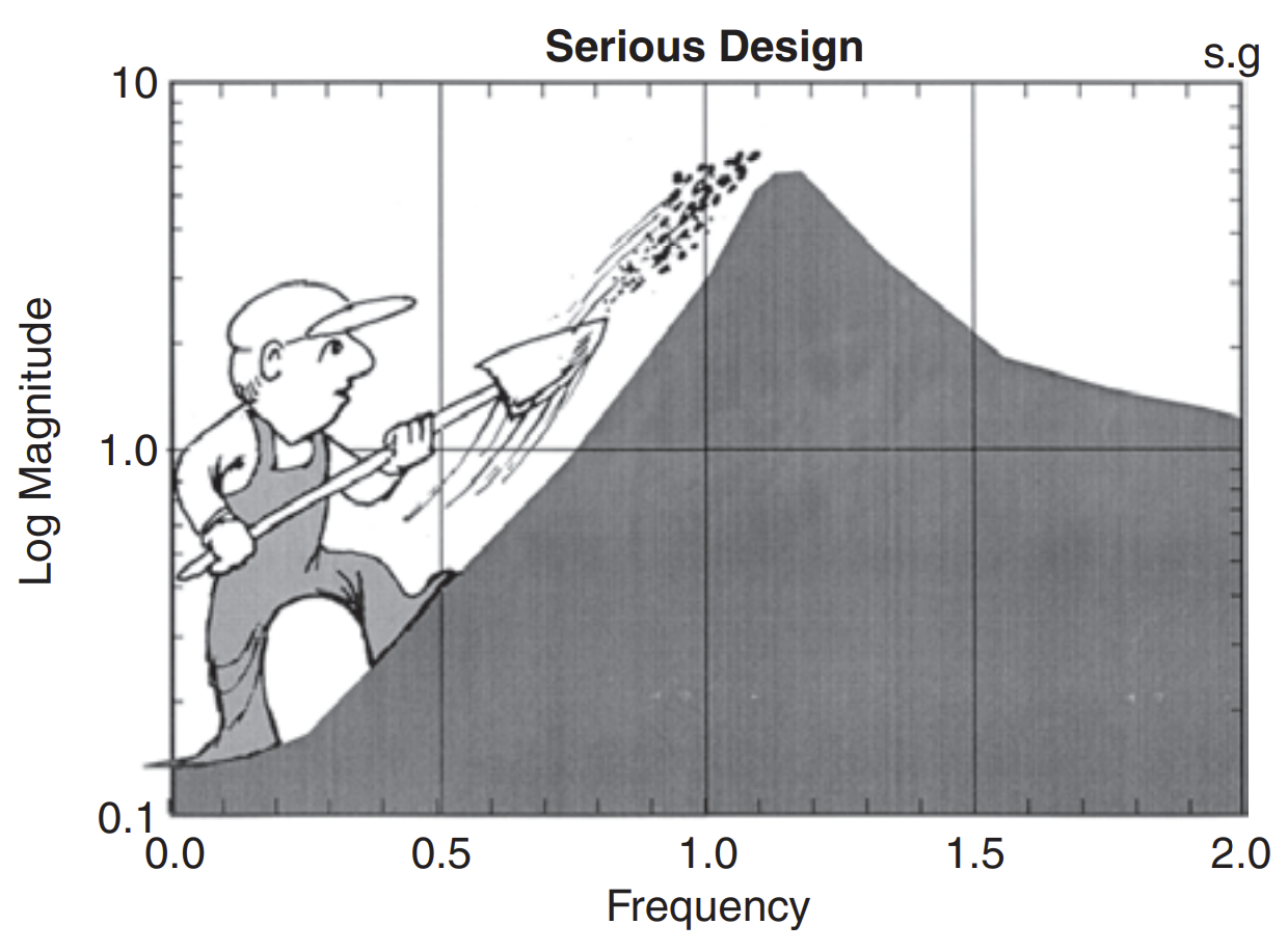
Figure 14 Timeless representation of Bode sensitivity integral. Reducing the sensitivity at lower frequency by shovelling the sensitivity to higher frequency! Image courtesy of Gunter Stein [7].
Typically, Bode sensitivity analysis is relevant for two types of closed-loop systems [1, 6]:
Open-loop transfer function has at least two more poles than zeros (open-loop of with relative degree of at least two).
Open-loop transfer function with an RHP-zero or time delay.
Considering that in most practical systems both the plant and controller are proper and the time delay is present, the Bode sensitivity analysis is almost always relevant.
Open-loop with the relative degree of two or more: Consider a rational open-loop transfer function with the relative degree of two or more and without RHP-zeros. In addition, suppose that open-loop transfer function has \(N_p\) RHP-poles denoted by \(p_i\). Then the closed-loop sensitivity transfer function must satisfy
where \(\Re{(p_i)}\) is the real part of the unstable pole. See [8] for proof.
Open-loop with RHP-zero: Consider a rational open-loop transfer function with a single RHP-zero \(z = x + j y\). In addition, suppose that open-loop transfer function has \(N_p\) RHP-poles denoted by \(p_i\). Then the closed-loop sensitivity transfer function must satisfy
where
See [8] for proof.
Note
According to the Bode sensitivity integral in (5), an RHP-zero located close to an RHP-pole will result in a large peak in sensitivity. Such configurations typically lead to systems that are practically uncontrollable. Moreover, this analysis advises against attempting to cancel an unstable pole in the plant with an RHP-zero from the controller, as it can lead to unstable system behavior.
Note
The weighting function \(f(z,\omega)\) in (6) reduces the contribution of \(\ln\|S\|\) at frequencies \(\omega \geq x\). This allows us to use the following version of (5)
Note that the Bode sensitivity integral mentioned above imposes stricter conditions than (4). This is due to the need to balance the frequency range where \(\|S\| \leq 1\) (indicating perfect control) against the range where \(\|S\| > 1\) (indicating poor control), within a finite frequency interval \([0, x]\). As a result, this balancing act can lead to larger peaks in \(S\).
The Bode sensitivity integral demonstrates that sensitivity peaks are unavoidable in practical applications, setting a fundamental limit on achievable performance and stability margins. Achieving perfect closed-loop set-point tracking and disturbance rejection at one frequency invariably leads to closed-loop performance that is worse than open-loop control at another frequency. In addition, there is an essential trade-off between the quality of reference tracking, disturbance rejection, and the stability margin of the closed-loop system, along with its transient response.
Robust Stability and Transient Performance: The maximum peak of sensitivity transfer function and complementary sensitivity transfer functions is defined as
Based on the algebraic constraint in (3) we have
indicating that at each frequency magnitude of \(S\) and \(T\) can differ at most by 1. Consequently \(M_s\) and \(M_T\) can differ by no more than 1. Subsequently, a large peak in sensitivity suggests a similar large peak in complementary sensitivity.
The large values of \(M_s\) and \(M_T\) indicate poor robustness and performance [1]. Specifically, a high \(M_T\) shows that measurement noise \(\eta\) is amplified at the frequency where the complementary sensitivity peaks. Similarly, a high \(M_S\) indicates poor regulation at the frequency of peak sensitivity. This relationship highlights how these metrics directly impact the system’s effectiveness in handling noise and disturbances.

Figure 15 The distance between the open-loop transfer function \(L(j\omega)\) and \(-1\) is equal to \(S^{\text{-}1}(j\omega)\). Hence, \(M_s^{\text{-}1}\) is closest distance between \(L(j\omega)\) and \(-1\) and direct indicator of robust stability. Furthermore, \(M_s\) provides lower-bounds for classical phase margin and gain margin.
In addition to performance, the peak sensitivity \(M_s\), serves as a direct measure of robust stability. Consider the Nyquist plot of the open-loop transfer function \(L(s)\), as shown in Figure 15. To maintain closed-loop stability, the number of encirclements of \(L(j\omega)\) around \(-1\) must not change. Therefore, it is crucial to keep \(L(j\omega)\) within a reasonable distance from \(-1\). The distance between \(L(j\omega)\) and \(-1\) is equal to the inverse of the sensitivity function \(\| S(j\omega) \|^{\text{-}1} = \|-1 - L(j\omega)\|\). Consequently, \(M_s^{\text{-}1}\) represents the minimum distance between \(L(j\omega)\) and \(-1\). Thus, a smaller \(M_s\) implies a greater distance from \(-1\), allowing greater uncertainty before instability occurs, thus improving the robustness margin [1, 6]. Furthermore, Figure 15 helps link peak sensitivity and peak complementary sensitivity with classical indicators of robust stability, namely Bode gain margin and phase margin as follow
Keeping \(M_s\) less than \(2\) guarantees a gain margin above \(6\) dB and a phase margin greater than \(30^\circ\).
Time domain |
Frequency domain |
||
|---|---|---|---|
Overshoot |
Total Variation |
\(M_T\) |
\(M_s\) |
1 |
1 |
1 |
1.05 |
1 |
1.01 |
1 |
1.2 |
1 |
1.13 |
1 |
1.3 |
1.18 |
1.44 |
1.18 |
1.5 |
1.27 |
1.76 |
1.42 |
1.7 |
1.37 |
2.18 |
1.74 |
2 |
1.49 |
2.91 |
2.31 |
2.5 |
1.56 |
3.57 |
2.82 |
3 |
1.72 |
6.32 |
4.97 |
5 |
Finally, the peak sensitivity \(M_s\) and peak complementary sensitivity \(M_T\) are reliable indicators of the closed-loop transient response. This concept is examined by crudely approximating the closed-loop complementary sensitivity function \(T(s)\) by the following second order system [1]
We evaluate the system’s transient response by focusing on overshoot and the total variation in the step response. The total variation (TV) is calculated as follows:
where \(g_T(t)\) is impulse response of \(T\). The total variation helps us to understand the degree of oscillation in the response.
Table 1 shows the total variation and overshoot for the step response of the second order closed-loop system in (7) for different values of \(M_S\) and \(M_T\). It can be observed that
This observation suggests that \(M_T\) serves as a reliable measure for assessing the quality of transient response in the time domain, using frequency domain peak complementary sensitivity.
Internal Stability: The closed-loop system in Figure 12 is stable if and only if the transfer functions \(T\), \(S\), \(SP\), \(KS\) are stable. Note that the internal stability of closed-loop depends on the stability of \(SP\) and not \(P\). This indicates the greatest benefit of feedback, where even for an unstable plant \(P\) we can still achieve stability as long as \(SP\) is stable [5].
To conclude this section, we will summarize the advantages of closed-loop systems and how they address the limitations of open-loop control, as discussed earlier [1].
No Need for Perfect Model: Achieving perfect set-point regulation in closed-loop control doesn’t necessitate a perfect model of the plant \(P\). In fact, closed-loop systems can inherently handle model inaccuracies and uncertainties, with the peak sensitivity \(M_S\) offering a way to gauge closed-loop robustness.
Invertibility Not Required: Closed-loop control systems do not require the plant \(P\) be invertible. However, non-invertible plants, due to RHP-zeros or delays, will limit the achievable bandwidth in the closed-loop system.
Stabilizing Unstable Plants: One of the key strengths of closed-loop systems is their ability to stabilize plants that would otherwise be unstable.
Disturbance Rejection without Measurement: Closed-loop systems can fully reject input disturbances without directly measuring them. However, to effectively counter disturbances, the controller should incorporate a disturbance model, adhering to the internal model principle (IMP).

Figure 16 Averaged model of three phase inverter interfaced to the grid. The inverter use a \(LC\) filter to smooth out the switching frequency harmonics and the transmission line is modeled as an \(RL\) impedance.
We have reviewed some of the core concepts of feedback control theory; now we are ready to cover the control of DC/AC inverters.
DC/AC Inverter Interface Setup
We study the control of the three-phase DC/AC inverter in the context of a system that involves two three-phase voltage sources, as illustrated in Figure 16. The inverter is modeled as three controlled voltage sources based on the averaged model of a half-bridge. The inverter’s output voltage is governed by the modulation signals \(\vv{m} = [m_{a}, m_{b}, m_{c}]^{\top}\), where \(m_{a}, m_{b}, m_{c} \in [-1,1]\). The inverter output, a voltage pulse train, is smoothed by a \(LC\) with an equivalent series resistor (ESR) \(R\). The voltage across the capacitor in the \(abc\) frame is denoted by \(\vv{v_{c}} = [v_{ca}, v_{cb}, v_{cc}]^{\top}\), and the current passing through \(L\) and \(R\) is represented by \(\vv{i_L} = [i_{La}, i_{Lb}, i_{Lc}]\). The voltage source \(\vv{v_{g}} = [v_{ga}, v_{gb}, v_{gc}]^{\top}\) represents the dynamics of external power entities such as the grid, the point of common coupling (PCC), or any other collective of DC/AC inverters. Since the specific behaviors of these external power systems are not precisely known, modeled, or change over time, we consider \(\vv{v_g}\) as an unknown quantity. Consequently, \(\vv{v}_g\) is treated as disturbances within our system analysis. The impedances \(R_g\) and \(L_g\) account for the characteristics of the transmission line, grid impedance (particularly for a weak grid), and the grid-side inductor of the \(LCL\) filter, if utilized.
The dynamics of the three-phase inverter, including the \(LC\) filter and the \(RL\) transmission line within, depicted in Figure 16 are
where the parameters \(L\), \(R\), \(C\), \(L_g\), and \(R_g\) are \(3 \times 3\) diagonal matrices. In these matrices, each diagonal entry represents the value of the parameter for the corresponding phase as shown below
In symmetric three-phase systems, these parameters are equal across all three phases [1].
The dynamics of the three-phase inverter in (8) are represented in the \(abc\) stationary frame. In the \(abc\) frame, the voltages, currents, and other electrical parameters of the three-phase system are represented as they are, without transformation. Each phase \(a\), \(b\), and \(c\) is treated individually, reflecting the actual sinusoidal waveform observed in three-phase real-world systems. \(abc\) frame is crucial for developing initial models and for systems where direct control or monitoring of each phase is required. However, to implement more sophisticated control strategies, transformed reference frames such as \(\alpha\beta\) and \(dq\) are used [1].
Important
Control of inverters in the \(\alpha\beta\) (stationary) and \(dq\) (rotating) reference frames is a critical aspect of power electronics, particularly in applications involving AC power systems. The \(\alpha\beta\) frame provides a way to transform three-phase AC signals into two-dimensional vectors, simplifying analysis and control by reducing the complexity of the system from three dimensions to two. The \(dq\) further refines this approach by introducing a rotating reference frame, essentially converting AC quantities into DC-like components, reducing the complexity of control design [1, 2]. A deep understanding of the three reference frames-\(abc\), \(\alpha\beta\), and \(dq\)-is rooted in the concept of the space phasor. Grasping the concept of phasor is crucial before exploring advanced control strategies, as it forms the foundational link among these reference frames. Therefore, before going any further in this section I suggest you review the concept of phasor provided in Space Phasor.
Dynamics in \(\alpha\beta\) and \(dq\) Frames
The initial modeling of power systems in the time domain is typically carried out in the \(abc\) frame, as this stationary frame naturally aligns with the per-phase characteristics of the system. However, to control the system in the \(\alpha\beta\) and \(dq\) frames, it is necessary to translate the dynamics into these frames. This involves a straightforward process where we employ the inverse Clarke transformation and the inverse \(dq 0\) transformation as a change of variables to convert the \(abc\) signals. The details of this approach will be clarified further in the upcoming discussion of inverter dynamics within the \(\alpha\beta\) frame.
Inverter dynamics in \(\alpha\beta 0\) stationary frame: Using the inverse Clarke transform, we can express \(abc\) variables with its corresponding \(\alpha\beta\) counterpart using the change of variable \(\vv{f_{abc}} = T_{\alpha\beta0}^{\text{-}1}\vv{f_{\alpha\beta}}\). Replacing all the \(abc\) variables in (8) with the corresponding \(\alpha\beta\) representation, we get the following inverter dynamics in the \(\alpha\beta 0\) frame
In symmetric three phase systems, the dynamics in the \(\alpha\beta\) simplifies to
Inverter dynamics in \(dq 0\) rotating frame: Using both the inverse Clarke transform and the \(dq\) to \(\alpha\beta\) transform \(\mathbf{R}(\theta_{dq})\), we can express any \(abc\) variable with its corresponding \(dq\) counterpart as \(\vv{f_{abc}} = T_{\alpha\beta0}^{\text{-}1}\mathbf{R(\theta_{dq})}\vv{f_{dq}}\). Subsequently, we get the following \(dq\) representation of the dynamical equation
Again, in case of symmetric three-phase systems, the above dynamics simplifies to
Note that unlike the dynamics in \(abc\) and \(\alpha\beta\) stationary frames, the \(dq\) dynamics are coupled.
Inverter Control
We discussed the DC/AC inverter’s interface with the power system as shown in Figure 16. Furthermore, we examined the concepts of phasors, the \(abc\), \(\alpha\beta\), and \(dq\) reference frames, and outlined the dynamics of DC/AC inverters in each of these frameworks. Now, we are ready to discuss the conventional methods typically employed in the literature to control DC/AC inverters. Although there exists a diverse array of control techniques for AC/DC inverters, the approach outlined in this section outline the most prevalent approach adopted in state of the art designs. However, we use some of the control formalism in Closed-Loop Control, specifically the sensitivity, in control design. This segment also serves to introduce traditional control strategies, setting the stage for contrasting these with our proposed methods in subsequent sections.
In this section, we will focus on the three most common operational modes of the DC/AC inverter: the current source inverter, the voltage source inverter, and the grid-forming inverter. Although DC/AC inverters can function in other modes, such as a static synchronous compensator (STATCOM) or as part of an energy storage system (ESS), understanding these primary modes is essential. This knowledge lays the groundwork for clarifying the control objectives and requirements applicable to the other operational modes as well. Following this, we explore the cascaded control architecture, which includes an inner current loop and an outer voltage loop in both the \(\alpha\beta\) and \(dq\) frames. We will discuss the control design strategies necessary to meet the control objectives for each operating mode while maintaining appropriate phase margins.
Cascaded Control Structure
Cascaded control is a hierarchical control structure that uses multiple layers of controllers, each with specific functions, to manage a complex process more effectively than a single controller could. Typically, these systems involve at least two control loops: an inner loop and an outer loop. The inner loop is designed to respond quickly and manage the fast dynamics of the system, often focusing on basic, direct control tasks such as current control in power systems. The outer loop operates at a lower bandwidth, handling objectives such as voltage control. This arrangement typically employs signals from outer loops, such as compensator output signal, as an input (set-point) for the inner loops. By separating control tasks into distinct layers that operate on different time scales, cascaded control systems can address complex control challenges effectively, which makes them especially useful in power electronics applications.

Figure 17 Common cascaded structure with inner current closed-loop and outer voltag loop. The output of voltage compensator \(K_v\) is the set-point to inner current closed-loop.
In the control of DC/AC inverters, it is common to employ cascaded control systems that feature a high-bandwidth inner current closed-loop for regulating inductor current and an outer voltage closed-loop for controlling capacitor voltage. In the following sections, we will provide a detailed control design and analysis for both the inner current loop and the outer voltage loop in \(\alpha\beta\) and \(dq\) frame.
Inner Current Loop
The inner current loop is at the core of the nested closed-loop architecture commonly used in inverter control. It is crucial to design the inner current controller to achieve the maximum possible bandwidth because a high-bandwidth inner loop is essential to ensure sufficient bandwidth in the outer loops. Additionally, a robust inner loop facilitates the implementation of safety features, such as maximum current limitation, which are critical for responding to fast fault transients. However, achieving high bandwidth in the inner loop can also introduce challenges related to maintaining robust stability in the system.

Figure 18 The closed-loop implementation for control of \(\alpha\) component of inductor current.

Figure 19 The closed-loop implementation for control of \(\beta\) component of inductor current. These two closed-loops are completely independent and decoupled from each other.
\(\boldsymbol{\alpha\beta}\) inner current loop: The inductor current dynamics in Laplace domain and \(\alpha\beta\) frame is
where \(G_i\) represent the indcutor dynamics in Laplace domain
In (10) the modulation signal \(\vv{\hat{m}_{\alpha\beta}}\) is the physical actuation signal and \(\vv{\hat{v}_{c\alpha\beta}}\) appears as an input disturbance to \(G_i\).
We attenuate the effect of the input disturbance, \(\vv{\hat{v}_{c\alpha\beta}}\), into the plant \(G_i\) by incorporating the capacitor voltage feedforward into the modulation signal
where \(\vv{\hat{u}_{i\alpha\beta}}\) is the output of the controller \(K_i\), see Figure 18 and Figure 19. Note that we have used \(\vv{\hat{m}_{\alpha\beta}^*}\) instead of \(\vv{\hat{m}_{\alpha\beta}}\) in (12) to account for the impact of delays from the DSP and PWM modulator on the closed-loop system. These delays arise from the sampling of control variables such as voltage and current, the computation of the control algorithm, and changes in the PWM output. To incorporate the effect of these delays into the closed-loop analysis, we consider \(\vv{\hat{m}_{\alpha\beta}}\) to be a delayed version of \(\vv{\hat{m}_{\alpha\beta}^*}\), that is
The transfer function \(G_d = e^{-T_d s}\) represent the transport delay between the sampling of the control signals until the realization of the PWM signal as shown in Figure 18. The value of transport delay \(T_d\) depends on several factors, such as the ADC sampling scheme and the PWM update scheme. However, in this work, we use a plausible value of \(T_d = 1.5 T_s\), where \(T_s\) is the sampling frequency.
Replacing the modulation scheme in (12) and effect of delay in (13) into (10), the open loop transfer function becomes
Closing the control loop using the feedback controller \(K_i\), we get the following closed-loop transfer functions between the input reference \(\vv{\hat{i}_{r\alpha\beta}}\), capacitor voltage \(\vv{\hat{v}_{c\alpha\beta}}\), and inductor current \(\vv{\hat{i}_{L\alpha\beta}}\) as
Writing above closed-loop transfer functions in terms of sensitivity and complementary sensitivity is advantageous. This approach leverages the detailed analysis available for the sensitivity transfer function, helping to clearly show the trade-offs between different control objectives. This method provides a clearer understanding of how changes in one aspect of system performance may affect others.
For the closed-loop transfer function in (14), the complementary sensitivity transfer function \(T_i\) and sensitivity transfer function \(S_i\) are given below
The closed-loop system in (14) in terms of sensitivity and complementary sensitivity is
It is important to understand that based on the definitions of sensitivity, \(S_i\), and complementary sensitivity, \(T_i\), as given in (15), there exists an algebraic constraint: \(S_i + T_i = 1\). Ideally, for precise setpoint tracking of \(\vv{\hat{i}_{r\alpha\beta}}\) and effective disturbance rejection of \(\vv{\hat{v}_{c\alpha\beta}}\), we would like \(T_i = 1\) and \(S_i = 0\). However, the Bode sensitivity integral imposes limitations on the frequency range over which \(S_i\) can be kept small.
Our control design approach initially assumes that the transport delay \(G_d\) in (15) is one. This simplification is necessary because \(G_d = e^{-T_d s}\), a transcendental function, cannot be represented by any finite-order transfer function. Furthermore, the inclusion of transport delay \(G_d\) only leads to unnecessary complication in loop-shaping control design. We propose the following fourth-order compensator \(K_i\) for inner closed-loop
In the above, \(\omega_c\) is the desired open-loop gain cross-over frequency, \(\omega_l\) is same as (11), \(\omega_f\) is the fundamental frequency (\(60\) Hz), and \(z_{\text{lead}}\) and \(p_{\text{lead}}\) represent the zeros and poles of lead compensator. The PI compensator in (17) provides adequate gain at low-frequency eliminating the DC bias and low frequency disturbances on the output sine waveform. The PR compensator in (17) provides infinite gain at fundamental frequency \(\omega_f\) ensuring both perfect set-point regulation and disturbance rejection. The damping parameter \(\zeta\) in PR compensator provides robustness to frequency deviation and can be designed using following formula
where \(\Delta \omega_g\) represents the grid frequency deviation from the nominal values \(\omega_f\). Finally, the lead compensator provides adequate phase margin at the fundamental frequency to counteract the phase lag introduced by the PR compensator. The zeros and poles of lead compensator are computed as
where \(\delta_f\) is the required phase margin typically \(50^\circ \leq \delta_f\). Figure 20 shows the inner current open-loop for various delay values. It is clear that at the same bandwidth \(\omega_c\), larger delay \(T_d\) results in a reduced phase margin. Furthermore, Figure 21 displays the closed-loop response, highlighting that a larger delay at the same closed-loop bandwidth results in a higher peak in complementary sensitivity \(M_T\). This higher peak suggests a poorer closed-loop resonant response, indicating less stability under these conditions.

Figure 20 Inner current open-loop in \(\alpha\beta\) frame. The PR compensator introduces large gain at the fundametnal frequency.

Figure 21 inner current closed-loop showing increased peak \(M_T\) for larger values \(T_d\).
The controller in (17) was designed under the assumption that there is no transport delay, essentially setting \(G_d = 1\). However, we demonstrate that this controller can still maintain appropriate gain and phase margins provided there is sufficient frequency separation between the open-loop bandwidth, \(\omega_c\), and the transport delay, \(T_d\). A useful rule of thump is to keep the maximum phase shift introduced by the delay at the open-loop gain crossover frequency lower than \(30^\circ\). This approach leads to the following formula for \(\omega_c\)
The upper-bound on the gain cross-over frequency \(\omega_c\) guarantees at least \(60^\circ\) phase margin.

Figure 22 Peak sensitivity for different \(\omega_c T_d\). For larger values of \(T_d\), we see an increase in the peak sensitivity.
Another useful perspective in control system analysis is to consider the peak sensitivity, denoted by \(M_s = \|S_i\|_\infty\). The peak sensitivity \(M_s\) serves as a direct indicator of the robust stability of the system. Typically, it is preferable to keep the peak sensitivity below 2, which means \(M_s = \|S_i\|_\infty \leq 2\). According to the Bode sensitivity integral, increasing the closed-loop bandwidth results in an increase in the peak sensitivity. This essentially provides an upper bound on the open-loop cross-over frequency \(\omega_c\), see Figure 22.
\(\boldsymbol{dq}\) inner current loop: The inductor current dynamics in Laplace domain and \(dq\) frame is
where \(G_i\) represent the same indcutor dynamics in (11). The inductor dynamic in the \(dq\) frame is similar to the \(\alpha\beta\) frame, detailed in (10), with the notable addition of a coupling term between the \(d\) and \(q\) axes dynamics. Using the same approach as applied in the \(\alpha\beta\) frame, we define the modulation signal to incorporate the feedforward coupling term in addition to the capacitor voltage, as follows (see Figure 23) :

Figure 23 The \(dq\) frame introduces additional coupling between the \(d\) and \(q\) axis. We can achieve decoupling by employing the feedforward compensation of the signals \(\{v_{cd},v_{cq}\}\) and \(\{L\dot{\theta}i_{Ld},L\dot{\theta}i_{Lq}\}\).
Including the coupling term in the above formulation allows us to achieve a significant decoupling effect between the dynamics of the \(d\) and \(q\) axes [1]. This is evident when we substitute \(\vv{\hat{m}_{dq}} = G_d \vv{\hat{m}_{dq}^*}\) into (18) to get
The residue of the coupling effect in the above equation can be formulated as a multiplicative perturbation of the nominal plant \(G_i\) as
The transfer function \(w_v\) above captures the effects of residual coupling, which arises from imperfect decoupling due to presence of DSP delay \(G_d\). It is defined as follows:
When the dynamics of the inductor \(G_i\) is significantly slower than the DSP time delay, specifically when \(\omega_l \ll 1/T_d\), it is reasonable to assume that the coupled perturbation is nearly negligible, that is, \(\omega_v \approx 0\).
We approach the inner closed-loop control design using the loop shaping method. However, unlike shaping the open loop, as we did in \(\alpha\beta\) frame, we directly shape the closed-loop. We aim to design the inner closed-loop, \(T_i\), as a first-order unity gain low-pass filter
where \(\omega_B\) represents the desired closed-loop bandwidth. Again, assuming that \(G_d = 1\), it is easy to validate that the following PI controller achieves the desired closed-loop shape
The above feedback controller is a simple PI compensator where the only design parameter is the closed-loop bandwidth \(\omega_B\). Ideally, we want \(\omega_B\) to be as high as possible, but the DSP delay imposes a limit on the maximum achievable bandwidth. To ensure that the phase delay caused by the DSP remains below \(30^\circ\), it is necessary to maintain the bandwidth within following limit

Figure 24 Peak sensitivity for different \(\omega_c T_d\). For larger values of \(T_d\), we see a increase in the peak sensitivity.
We can also approach the maximum inner loop bandwidth using the peak sensitivity argument. In Fig. Figure 24 we sketched the peak sensitivity resonance for different ratios of closed-loop bandwidth to DSP delay.
Outer Voltage Loop
The main goal of the outer voltage loop is to maintain the capacitor voltage at a desired set-point by controlling the current flow into the capacitor.
\(\boldsymbol{\alpha\beta}\) outer voltage loop: The total current flowing into the capacitor comprises two components: \(\vv{\hat{i}_{L\alpha\beta}}\) and \(\vv{\hat{i}_{g\alpha\beta}}\) as outlined in (9). Although \(\vv{\hat{i}_{L\alpha\beta}}\) can be controlled through the inner current closed-loop, \(\vv{\hat{i}_{g\alpha\beta}}\) acts as an input disturbance that cannot be directly controlled. By substituting \(\vv{\hat{i}_{L\alpha\beta}}\) in (9) with the expression from (16), we can effectively manage the overall current dynamics to achieve the desired voltage regulation.

Figure 25 The outer voltage closed-loop formed around the inner current closed-loop indicated by \(T_i\). The \(\alpha\) and \(\beta\) voltage loop as shown above are independent.
To attenutae the effect of disturbance \(\vv{\hat{i}_{g\alpha\beta}}\) we define the current setpoint as
where \(\vv{u_{v\alpha\beta}}\) is the output of the voltage compensator and \(\vv{\hat{i}_{g\alpha\beta}}\) is the feedforward measurement of the grid current as shown in Figure 25. The closed-loop transfer function between the voltage setpoint \(\vv{\hat{v}_{r\alpha\beta}}\), current disturbance \(\vv{\hat{i}_{g\alpha\beta}}\), and capacitor voltage \(\vv{\hat{v}_{c\alpha\beta}}\) is
In above closed-loop, \(w_v = S_i G_i (1 - G_d) / K_v\), captures the effect capacitor feedforward compensation, \(S_i G_i (1 - G_d)\) in (20), as a multiplicative perturbation \(w\). This formulation allows us to represent the closed-loop in (21) in a simpler nominal form below
For the closed-loop transfer function in (21), the complementary sensitivity transfer function \(T_v\) and sensitivity transfer function \(S_v\) is given below
The closed-loop system in (14) in terms of sensitivity and complementary sensitivity is
We propose the following voltage compensator
In the above, \(\omega_v\) is the desired open-loop gain cross-over frequency, \(z_{\text{lag}}\) is the zero of PI compensator, \(\omega_f\) is the fundamental frequency (\(60\) Hz), and \(z_{\text{lead}}\) and \(p_{\text{lead}}\) represent the zeros and poles of lead compensator. The PI compensator in (22) provides adequate gain at low frequencies, eliminating the DC bias and low frequency disturbances on the output sine waveform. However, care should be taken such that \(z_{\text{lag}} \ll \omega_f\) to avoid excessive phase lag at PR resonant frequency. The PR compensator in (17) provides infinite gain at fundamental frequency \(\omega_f\) ensuring perfect voltage regulation and disturbance rejection at fundamental frequency. The damping parameter \(\zeta\) in PR compensator allows the voltage frequency to change within the following interval.
The lead compensator provides an adequate phase margin at the fundamental frequency to counteract the phase lag introduced by the PR compensator. The zeros and poles of the lead compensator are computed as
where \(\delta_f\) is the required phase margin typically \(50^\circ \leq \delta_f\).
To determine the outer open-loop bandwidth \(\omega_v\), it is important to consider that \(\omega_v\) is constrained by the phase delay \(T_d\) and the inner open-loop bandwidth \(\omega_c\). It is essential to select a \(\omega_v\) that ensures the peak sensitivity \(M_s\) for \(S_v\) remains below 2. Figure 28 shows how the peak sensitivity varies with different values of \(T_d\) and the ratio of outer to inner open-loop bandwidths \(\omega_v/\omega_c\). The results clearly show that a larger bandwidth separation between the inner and outer loops and a smaller delay \(T_d\) lead to a lower peak \(M_s\), enhancing the system’s robustness and transient response. In addition we have provided the sketch of complementary sensitivity in Figure 30 and Figure 31.

Figure 26 Peak sensitivity \(M_s\) for \(\omega_v/\omega_c = 0.8\).

Figure 27 Peak sensitivity \(M_s\) for \(\omega_v/\omega_c = 0.6\).

Figure 28 Peak sensitivity \(M_s\) for \(\omega_v/\omega_c = 0.5\).

Figure 29 Peak complementary sensitivity \(M_T\) for \(\omega_v/\omega_c = 0.8\).

Figure 30 Peak complementary sensitivity \(M_T\) for \(\omega_v/\omega_c = 0.6\).

Figure 31 Peak complementary sensitivity \(M_T\) for \(\omega_v/\omega_c = 0.5\).
\(dq\) outer voltage loop: We design the \(dq\) outer voltage loop by adopting similar approach as discussed for \(\alpha\beta\) outer voltage loop. The capacitor voltage dynamics in the \(dq\) frame is given below
The above capacitor voltage dynamic is similar to \(\alpha\beta\) capacitor dynamics, plus the coupling term between the \(d\) and \(q\) dynamics. To achieve decoupling and also attenuate the effect of current disturbance \(\vv{\hat{i}_{gdq}}\), we define the current reference as follow (see Figure 32):

Figure 32 The outer voltage closed-loop formed around the inner current closed-loop indicated by \(T_i\). The \(d\) and \(q\) voltage loop as shown above are coupled.
This results in the following capacitor voltage dynamics
where \(\vv{u_{vdq}}\) is the output of the voltage compensator. The closed-loop transfer function between the voltage setpoint \(\vv{\hat{v}_{rdq}}\), current disturbance \(\vv{\hat{i}_{gdq}}\), and capacitor voltage \(\vv{\hat{v}_{cdq}}\) is
In above closed-loop \(w_v\), captures the effect capacitor feedforward compensation, \(S_i G_i (1 - G_d)\) in (23), and the decoupling residue term in (24). These influences are characterized as a multiplicative perturbation \(w_v\), as follows:
Typically, for high-bandwidth inner closed-loop the above perturbation is negligble \(w_v \approx 0\). This allows us to represent the closed-loop in (25) in a simpler nominal form below
where the sensitivity \(S_v\) and complementary sensitivty \(T_v\) are define below
For the given voltage closed-loop we propose following PI controller
where \(\omega_v\) is the desired voltage open-loop bandwidth, \(C\) is the value of filter capacitor, and \(z_{\text{lead}}\) is the compensator zero. The PI compensator has two tunable parameters, \(\omega_v\) and \(z_{\text{lead}}\), and the corresponding open-loop is given as
where we replaced \(T_i\) from (19). We choose the values of \(\omega_v\) and \(z_{\text{lead}}\) such that the open-loop attains the maximum phase margin of \(\delta_c\) at gain cross-over frequency \(\omega_v\). This method, known as the symmetrical optimum [1], effectively fixes both \(\omega_v\) and \(z_{\text{lead}}\) as
where \(\omega_B\) is the same as the inner current closed-loop in (19). For values of \(50^\circ \leq \delta_c\) the corresponding voltage outer loop shows satisfactory stability margins and performance characteristics.
Inverter Operation Modes
Having thoroughly discussed the control design for cascaded control, we will now explore three of the most common operation modes of DC/AC inverters in terms of cascaded control.
Current Source Inverters
Current source inverters, also known as grid following inverters (GFL), are currently the most prevalent type of DC/AC inverters. GFL inverters are essential component in renewable energy systems, particularly photovoltaic systems and wind turbines, where they play a pivotal role in interfacing stochastic renewable energy sources with the stable utility grid [1, 2]. This type of inverter synchronizes its output with the grid’s voltage waveform, effectively “following” the grid’s voltage. In addition, grid-following inverters often include features like maximum power point tracking (MPPT), which optimizes power conversion efficiency in photovoltaics and wind turbines.
Here are some of the key performance metrics commonly used for GFL inverters:
Power quality: Includes several sub-metrics such as total harmonic distortion (THD) in the output current, which should be kept low to avoid damaging the grid connected devices. Grid-following inverters must maintain a clean, sinusoidal waveform [11].
Dynamic response: The ability of the inverter to respond quickly to changes in load or other grid conditions is crucial. This includes how quickly the inverter can adjust its output to match the frequency and voltage variations in the grid [1].
Frequency synchronization: Since grid-following inverters synchronize their frequency with that of the grid, their ability to maintain this synchronization under dynamic conditions is a critical performance metric [12, 13].
Fault ride-through capability: This refers to the inverter’s ability to continue operating and support the grid during transient fault conditions without disconnecting or ceasing to operate [14].
It goes without saying that all the mentioned performance metrics must be met while also maintaining adequate stability margins. This becomes particularly crucial in conditions of a weak grid, where the grid impedance is prone to significant change.
Implementation of current sourced inverter: The basic implementation of a current source inverter requires only the inner current closed-loop, as illustrated in Figure 18 and Figure 19 for the \(\alpha\beta\) frame and Figure 23 for the \(dq\) frame. In this context, we only need to adjust the input set-points to the corresponding inner closed-loop based on the desired active and reactive power.
Based on the power calculations in the \(\alpha\beta\) frame, outlined in (39), the current set-point for the desired active and reactive power is determined as follows:
where \(P_0\) and \(Q_0\) represent the desired active and reactive power set-points.
To fully leverage the benefits of the \(dq\) rotating frame for a current sourced inverter, it is essential to first employ a Phase-Locked Loop (PLL) mechanism. This synchronizes and aligns the \(dq\) rotating frame with the voltage phasor, where \(v_q = 0\) and \(v_d = \|v\|\). Consequently, in this scenario, the \(dq\) current set-points are simply determined using the following simplified version of (40):
The key distinction between operating the current set-point in the \(\alpha\beta\) frame and the \(dq\) frame lies in the nature of the set-point signal. In the \(\alpha\beta\) frame, for constant power set-points, the current references \(\{i_{r\alpha},i_{r\beta}\}\) will mimic the sinusoidal shape of the measured voltages \(\{v_{\alpha},v_{\beta}\}\). In contrast, in the \(dq\) frame with constant power set-points, the current set-points \(\{i_{rd},i_{rq}\}\) themselves remain constant.
Voltage Source Inverters
DC/AC inverters designed as ideal voltage sources are a fundamental part of uninterruptible power supply (UPS) and backup power supplies. The “voltage source” aspect refers to the inverter’s ability to maintain a consistent frequency and voltage output regardless of changes in load conditions. This capability is crucial to ensure stable and reliable power delivery in the absence of a reliable power grid [1].
In theory, an ideal voltage source inverter would deliver a perfect sinusoidal output with no distortion, without any drop in output voltage under load change. In practical applications, while actual inverters cannot achieve these ideal conditions, voltage source inverters strive to closely approximate this behavior.
Ideal voltage source inverters are particularly valuable in applications where power quality is critical. They are used to ensure that sensitive electronic devices operate smoothly without the risk of damage from fluctuations in power. However, a major limitation of these inverters is their inability to be easily paralleled or share the load with other voltage source inverters, nor can they connect to the grid.
Here are some of the key performance metrics commonly used for GFL inverters:
Power quality: Total harmonic distortion (THD) in the output voltage should be kept low to avoid damaging the loads. The voltage source inverters must maintain a clean sinusoidal voltage of fundamental frequency (\(60\) Hz) [1].
Dynamic response: The ability of the inverter to respond quickly to changes in load. This includes how quickly the inverter can recover from voltage or frequency deviation in the face of sudden changes in the load profile [1].
Fault ride-through capability: Like GFL inverter, the voltage source inverter should continue operating during transient fault conditions without disconnecting or ceasing to operate.
As previously mentioned, voltage source inverters are designed to emulate ideal voltage sources, which can lead to poor performance when they are paralleled with other ideal voltage sources such as the grid or other voltage source inverters. Grid-forming inverters (GFM) resolve this issue by incorporating droop control, which allows multiple inverter units to share the load effectively. This feature enables inverters to regulate both voltage and frequency, effectively creating and maintaining a small-scale grid.
Implementation of voltage source inverter: Implementation of a voltage source inverter requires use of the full cascaded structure with outer votlage loop and inner current closed-loop, as illustrated in Figure 25 for the \(\alpha\beta\) frame and the Figure 32 for the \(dq\) frame. In this context, we need to adjust the input set-points to the outer voltage closed-loop based on the desired voltage magnitude of frequency.
In the \(\alpha\beta\) frame this is simply achieved by calculating the voltage set-points for the \(\alpha\) and \(\beta\) voltage closed-loops as
where \(v_0\) and \(\omega_0\) is the deisred voltage magnitude and frequency.
In the \(dq\) frame, this can be easily accomplished by setting the voltage set-points for the \(d\) and \(q\) voltage loops and generating the phase angle for the \(dq\) frame as follows:
Again \(v_0\) is the desired voltage magnitude and \(\omega_0\) represents the desired voltage frequency.
Grid Forming Inverters
Grid-forming inverters are pivotal in the large-scale integration of renewable sources such as solar and wind in the absence of a viable grid. Unlike traditional grid-following inverters, which rely on the presence of a stable grid frequency to operate, grid-forming inverters form a viable islanded grid by regulating the frequency and voltage at their common PCC [15]. This capability makes them particularly valuable for systems with high levels of renewable penetration, where fluctuations in power output of the grid following inverters can challenge the stability of the conventional grid.
GFM inverters are designed to mimic the drooping characteristics of conventional synchronous generators, providing essential grid services such as voltage control, frequency regulation, and inertia [4, 15]. This not only helps form viable grid, but supports black start capabilities.
The droop control method enables stable and autonomous operation of parallel inverters without the need for direct communication between them. This method is essential in applications such as microgrids where multiple generating units operate together. Technically, droop control modifies the frequency and voltage set-points of voltage source inverter based on changes in load or generation, thereby mimicking the behavior of conventional synchronous generators.
The principle behind droop control lies in its characteristic equations, typically expressed as [15]
where \(\{\omega_0,v_0\}\) represent the nominal frequency and voltage, \(\{k_p, k_q\}\) are the droop coefficients, and \(\phi_z\)is the angle of the transmission line impedance. \(\{P_0,Q_0\}\) denote the nominal operating power, while \(\{P,Q\}\) are the measured output power of the inverter. Selecting the appropriate droop coefficients is crucial because it directly impacts how sensitive the inverter’s voltage and frequency are to changes in load, as well as the overall stability of the system [4].
The GFM control take different forms such as simple droop [16], virtual synchronous machine (VSM) [17], and virtual oscillator-based control (VOC) [18]. These control strategies, although different in their implementations and dynamics, imitate the drooping characteristics of the synchronous machine (SM) at a steady-state [19]. The invariable dependence of the GFM control strategies on the steady-state droop laws stems from the fundamental power flow equation
that associates the power flow through the impedance \(Z\angle \phi_z\), to corresponding terminal voltage magnitudes \(\{\|v_c\| ,\| v_g \| \}\), and phase difference \(\delta\) as one shown in Figure 54.
Droop control helps in proportionally sharing load among inverters according to their droop coefficients and improves the system’s ability to respond dynamically to changes in load without overloading individual units. It also helps to avoid the need for a central controller or extensive communication infrastructure, which can be a major advantage in decentralized systems.
Implementation of droop operated inverter: Implementation of a droop operated inverter, also known as grid forming, requires use of the full cascaded structure with outer voltage loop and inner current closed-loop, much like voltage source inverter. In this context, we need to adjust the input set-points to the outer voltage closed-loop based on drooping characteristics of voltage and frequency provided by the droop law in (26).
In the \(\alpha\beta\) frame this is simply achieved by calculating the voltage set-points for the \(\alpha\) and \(\beta\) voltage closed-loops as
The voltage set-points calculated above resemble those of an ideal voltage source inverter, with the key difference being that the voltage magnitude \(v_{\text{droop}}\) and frequency \(\omega_{\text{droop}}\) are not fixed. Instead, they are dynamically calculated using the droop law, as defined in (26), based on power calculations.
In the \(dq\) frame, the drooping characteristics is implemented by setting the voltage set-points for the \(d\) and \(q\) voltage loops and generating the phase angle for the \(dq\) frame as follows:
In this case \(v_{\text{droop}}\) directly sets the voltage magnitude \(v_{rd}\) while the \(dq\) angle, \(\theta_{dq}\), is calculated based on the drooped frequency \(\omega_{\text{droop}}\).
Sigurd Skogestad and Ian Postlethwaite. Multivariable feedback control: analysis and design, pages 15–62. john Wiley & sons, 2005.
Qing Liu, Tommaso Caldognetto, and Simone Buso. Review and comparison of grid-tied inverter controllers in microgrids. IEEE Transactions on Power Electronics, 35(7):7624–7639, 2019.
Amirnaser Yazdani and Reza Iravani. Voltage-sourced converters in power systems: modeling, control, and applications. John Wiley & Sons, 2010.
Robert H Lasseter, Zhe Chen, and Dinesh Pattabiraman. Grid-forming inverters: a critical asset for the power grid. IEEE Journal of Emerging and Selected Topics in Power Electronics, 8(2):925–935, 2019.
John C Doyle, Bruce A Francis, and Allen R Tannenbaum. Feedback control theory. Courier Corporation, 2013.
Kemin Zhou and John Comstock Doyle. Essentials of robust control. Volume 104. Prentice hall Upper Saddle River, NJ, 1998.
Gunter Stein. Respect the unstable. IEEE Control systems magazine, 23(4):12–25, 2003.
James Scott Freudenberg and Douglas Paul Looze. Frequency domain properties of scalar and multivariable feedback systems. Springer, 1988.
Mohammad Ebrahimi, Sayed Ali Khajehoddin, and Masoud Karimi-Ghartemani. Fast and robust single-phase $ dq $ current controller for smart inverter applications. IEEE transactions on power electronics, 31(5):3968–3976, 2015.
Aleksandr Reznik, Marcelo Godoy Simões, Ahmed Al-Durra, and SM Muyeen. $ lcl $ filter design and performance analysis for grid-interconnected systems. IEEE transactions on industry applications, 50(2):1225–1232, 2013.
Ahmad Tavakoli, Sajeeb Saha, Mohammad Taufiqul Arif, Md Enamul Haque, Nishad Mendis, and Aman MT Oo. Impacts of grid integration of solar pv and electric vehicle on grid stability, power quality and energy economics: a review. IET Energy Systems Integration, 2(3):243–260, 2020.
Kyoung-Jun Lee, Jong-Pil Lee, Dongsul Shin, Dong-Wook Yoo, and Hee-Je Kim. A novel grid synchronization pll method based on adaptive low-pass notch filter for grid-connected pcs. IEEE transactions on industrial electronics, 61(1):292–301, 2013.
Saeed Golestan, Mohammad Monfared, Francisco D Freijedo, and Josep M Guerrero. Dynamics assessment of advanced single-phase pll structures. IEEE transactions on industrial electronics, 60(6):2167–2177, 2012.
Aslan Mojallal and Saeed Lotfifard. Enhancement of grid connected pv arrays fault ride through and post fault recovery performance. IEEE Transactions on Smart Grid, 10(1):546–555, 2017.
Dayan B Rathnayake, Milad Akrami, Chitaranjan Phurailatpam, Si Phu Me, Sajjad Hadavi, Gamini Jayasinghe, Sasan Zabihi, and Behrooz Bahrani. Grid forming inverter modeling, control, and applications. IEEE Access, 9:114781–114807, 2021.
Peter Unruh, Maria Nuschke, Philipp Strauß, and Friedrich Welck. Overview on grid-forming inverter control methods. Energies, 13(10):2589, 2020.
Jia Liu, Yushi Miura, and Toshifumi Ise. Comparison of dynamic characteristics between virtual synchronous generator and droop control in inverter-based distributed generators. IEEE Transactions on Power Electronics, 31(5):3600–3611, 2015.
Brian B Johnson, Sairaj V Dhople, Abdullah O Hamadeh, and Philip T Krein. Synchronization of parallel single-phase inverters with virtual oscillator control. IEEE Transactions on Power Electronics, 29(11):6124–6138, 2013.
Brian Johnson, Miguel Rodriguez, Mohit Sinha, and Sairaj Dhople. Comparison of virtual oscillator and droop control. In 2017 IEEE 18th Workshop on Control and Modeling for Power Electronics (COMPEL), 1–6. IEEE, 2017.